Nitrides Seminar - Nate Palmquist
Attend in person at ESB 1001!
Zoom option also available
https://ucsb.zoom.us/j/81532609452?pwd=dmVIdTd0UTAvRlg3ekhjUnRHQ1dtQT09
Meeting ID: 815 3260 9452
Passcode: 334765
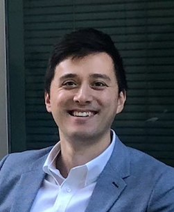
Nathan Palmquist
Graduate Student Researcher, Nakamura Group
University of California, Santa Barbara
Long Cavity m-plane GaN VCSELs utilizing a topside curved mirror
Recently, ultra-long cavity GaN VCSELs have been demonstrated that show low threshold currents and high output powers. The long cavity provided superior thermal stability and reduced processing constraints. Lateral mode control was provided by a curved lens etched into the bottomside of the device, which prevented diffraction and scattering loss from dominating device characteristics. To form their lens, they had to polish the substrate down to a thickness of approximately 20µm, increasing processing complexity. It is beneficial to place the lens on top of the VCSEL cavity without needing to lap or polish the substrate down to the desired cavity thickness. We introduce a cavity structure wherein the curved mirror is placed on the topside of the device, and the active region is placed far from the planar DBR and near the curved lens.
In addition to the topside mirror, we incorporate a nanoporous GaN (NP) DBR as our planar mirror. NP DBRs offer an epitaxial DBR option for GaN VCSELs with greater index contrast compared to conventional epitaxial DBRs (AlInN/GaN, AlGaN/GaN), and offer simpler processing compared to conventional dual dielectric DBR designs. However, prior NP DBR VCSELs suffer from high threshold currents and poor thermal performance that have prevented CW lasing for previous demonstrations. Our long cavity design enables our VCSELs to lase under CW conditions, with rollover dominated by the high voltage of the buried tunnel junction.