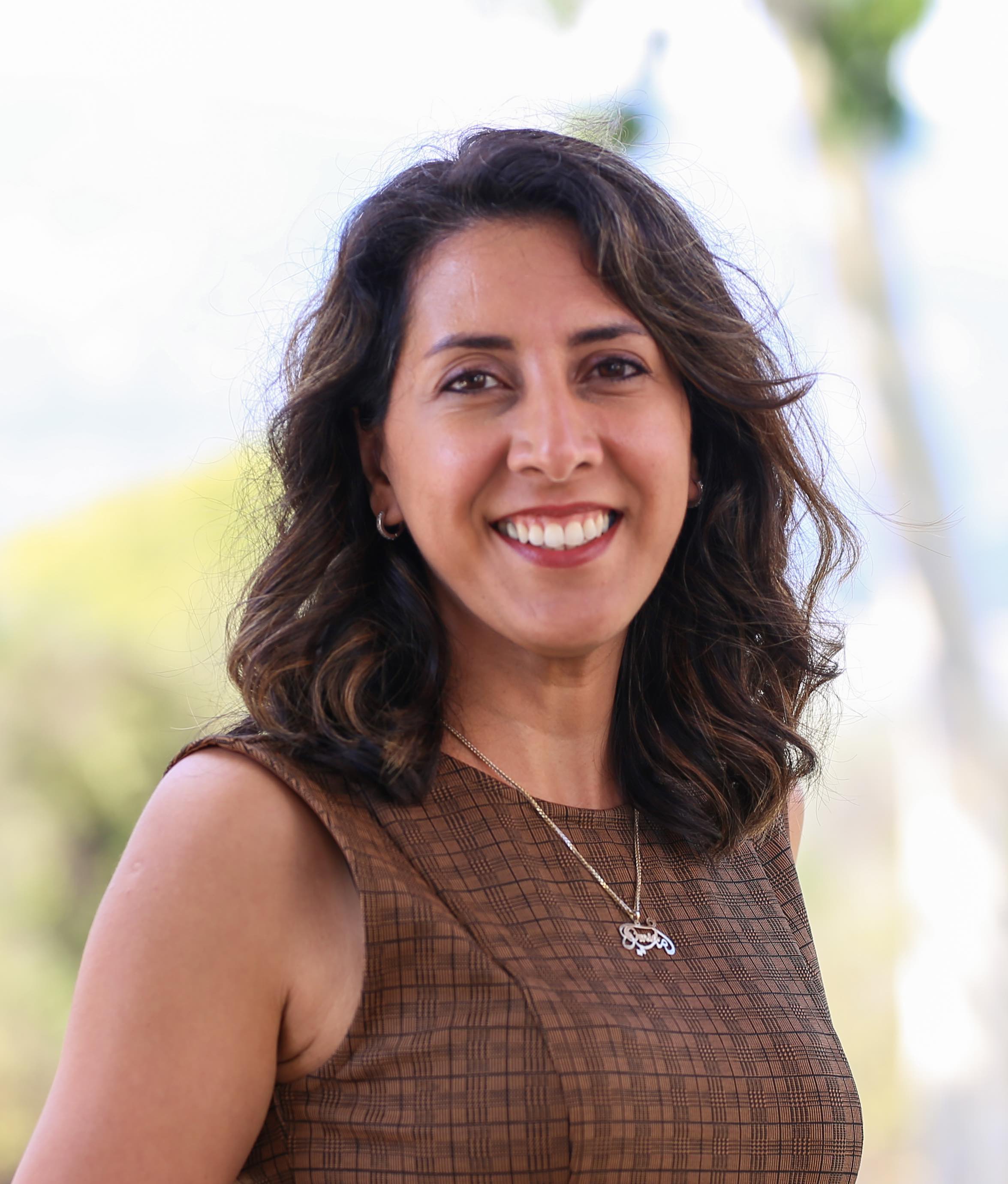
Elaheh Ahmadi Brings Mid-Career Experience to the ECE Faculty
Tuesday, October 21, 2025
by James Badham
Elaheh Ahmadi, who earned her PhD in the lab of Umesh Mishra, now dean of The Robert Mehrabian College of Engineering at UC Santa Barbara, returned to campus this past July as a mid-career professor in the Electrical & Computer Engineering Department. Previously, she held faculty positions at the University of Michigan and UC Los Angeles, following a period of postdoctoral research in the labs of Mishra and UCSB materials professor James Speck.
Ahmadi's research will sound familiar to anyone who knows the College of Engineering, as it is focused on epitaxial growth, device design, fabrication and characterization of nitrides for electronics, optoelectronics, and quantum applications.
She has received several awards of distinction, including an NSF Early CAREER Award, the Air Force Office of Scientific Research (AFOSR) and the Office of Naval Research (ONR) Young Investigator Program Awards, the DARPA Young Faculty Award, and a Presidential Early Career Award for Scientists and Engineers (PECASE) award the highest award for a young faculty member given by the U.S. government. We spoke with her in September.
Q: What led you to return to UCSB?
A: There are several reasons, both personal and professional. First, in my opinion, UCSB is the place to work on compound semiconductors, given the superb faculty, student, and staff researchers here; all the advanced shared instrumentation; and, most importantly, the DNA of collaboration. Together, these components have bred a strong culture that contributes tremendously to shaping the future of compound semiconductors.
UCSB also feels kind of like my second home. It was my first place I lived in the U.S. Travel restrictions did not allow me to return to Iran to visit my parents while I was in school, so, for seven years, I was only here. It’s where I built my friendships and my network. I have so many good memories from that time.
On both a personal and a professional level, it feels great to be back. Even when I was at UCLA, I used the UCSB Nanofabrication Facility heavily, relying on it to make progress. It’s a superb facility, evidenced by researchers who use it from industry, from other UCs, and from entities across the country and even around the world.
Q: Can you speak a bit more about the science component of your decision to return to UCSB, given your focus on compound semiconductors?
A: UCSB has achieved an enviable critical mass in compound semiconductors, with many different faculty members working in the same domain, leading to research overlaps that make it easy for people to work really nicely together to achieve breakthroughs in III-V materials. It makes UCSB unique, and it is how [professors emeriti] John Bowers and Larry Coldren, Umesh Mishra, materials professors Steve DenBaars and Jim Speck, electrical engineering professor Mark Rodwell, and so many others have been able to have such a major impact. I discovered that you can do a lot by yourself in semiconductors, but to have lasting impact requires more than one person. That's important, and it’s what I discovered at UCSB.
Q: What were some of the important takeaways from the time you spent earning your PhD in Dean Mishra’s lab?
A: I spent four years in Umesh’s group, which was very diverse and highly collaborative — and then two more years as a postdoc working between him and Jim Speck in materials. Again, it comes back to that collaborative culture which allowed me to gain knowledge in a breadth of fields within compound semiconductors and knowledge about how to choose a problem and succeed. Years later, in my current position, the relationships I built while pursuing my PhD here remain super important. It helps to have that network to form new collaborations, both on campus and with partners in industry.
Q: You return to UCSB having been named only the second recipient of the Mehrabian Career Development Chair, one of seventeen chairs endowed by the man who has recently lent his name to the College of Engineering. How does that land for you?
A: First, I greatly appreciate this honor. I know that Robert Mehrabian has done so much for the College of Engineering and that he has continued to support it, now by lending his name to it. The Career Development Chair will be a great benefit to me as a mid-career faculty member. The discretionary funding allows me to explore new ideas that might be higher risk and more difficult to find funding for. That, I think, is huge.
Q: Gallium nitride [GaN] has played a central role in a great deal of COE research, ever since (materials professor and Nobel laureate) Shuji Nakamura used it to create the blue LED, which, we all know, enabled the white LED, which revolutionized lighting around the world. How do you see that nexus of GaN and the College of Engineering?
A: GaN has become crucial to so many important opto-electronic applications, thanks to all the work done by people like Shuji and others. On the electronics side, which has been the focus of my research, wide-band-gap materials allow us to go to a higher power, whether in radio-frequency [RF] applications for radar, for 5G base stations, or for power electronics, which are all increasingly based on [GaN] transistors. Integrating gallium nitride with emerging compatible ferroelectric materials such as scandium aluminum nitride (ScAlN) will enable us to do things we have not thought about before.
GaN makes it possible to go to higher frequencies, which means that the passive elements, such as capacitors and inductors, can all become much smaller, making the products they are part of correspondingly smaller and more efficient. Now, new applications are emerging — in quantum, for instance — around other novel nitrides, such as niobium nitride [NbN], a low-temperature superconductor.
Q: Why that mix of gallium nitride with these other new materials?
A: Amorphous ferroelectric materials such as hafnium zirconium oxide are widely used with silicon. The ferroelectric nature of ScAlN allows one to explore the value of an epitaxial ferroelectric material in novel electronics such as memory. Its full potential can only be recognized by sustained research.
UCSB is the place to work on quantum, with the strong engagement of companies like Google and Microsoft, so I’m hoping that new collaborations will arise. Another new direction for my research is to pursue novel devices with neuromorphic functionalities, using nitride heterostructures, to enable more efficient, sustainable AI and deep-learning applications.
Q: Regarding your research, are there any immediate or longer-term challenges you face or goals that you have in mind as you start your lab here?
A: We've been getting some great results on several fronts, including those related to nitrogen-polar GaN transistors. I’m also excited about new areas of research, such as the previously mentioned efforts in quantum and sustainable AI. There are, of course, challenges with experimental work, from getting the lab set up to, now, the changes in federal funding, which will probably be the main challenge moving forward. But I'm really excited about being at UCSB, with all of the great support it provides. The MBE [molecular beam epitaxy] lab here is world renowned, and the lab manager, Kurt Olsen, is an invaluable resource. Though we find ourselves in a difficult time, I am confident that we will succeed because of the UCSB way.