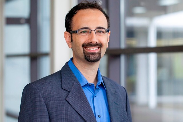
Special Nitrides Seminar - Dr. Stefano Leone, Fraunhofer Institute for Applied Solid State Physics IAF
Special Nitrides Seminar
Friday, January 31, 2025, 2:00PM
Attend in person at ESB 2001!
Zoom option also available
Meeting ID: 864 4261 9758 Passcode: 159421
Dr. Stefano Leone
MOCVD of AIScN and AIYN: growth and applications
Fraunhofer Institute for Applied Solid State Physics IAF
Tullastrasse 72, 79108
Freiburg, Germany
HOST: Dr. Stacia Keller
The increasing demand for reliable electronic components has spurred the exploration of novel materials. Nitride semiconductors stand out, particularly Scandium (Sc) and Yttrium (Y) alloys with wurtzite-AlN. These non-centrosymmetric crystals possess enhanced piezoelectric properties, making them promising candidates for various applications, such as high electron mobility transistors (HEMTs), and ferroelectric non-volatile memories.
The unique properties of AlScN and AlYN stem from the valence electrons in d orbitals and the large ionic radius of Sc, and Y. AlScN (18% Sc) and AlYN (11% Y) achieve a lattice matching with GaN. These features bring several benefits compared to their AlGaN/GaN counterparts, such as higher sheet carrier density and, presumably, higher transistor reliability. Innovative precursors heated at 90–150 ˚C enable depositing high-quality epitaxial layers of AlScN and AlYN in a commercial MOCVD reactor. The effect of the main growth parameters and several precursors for Sc and Y will be briefly discussed.
Higher vapor pressure enables deposition at higher growth rates, implicating several benefits but partially counterbalanced by higher impurities incorporation. The effect of growth rate and impurities on the structural and electrical characteristics of the layers will be discussed and explained with insights on structural characterization such as high-resolution TEM, XRD, and ToF-SIMS analysis, as well as electrical characteristics ranging from low-temperature Hall of 2DEGs in AlScN/GaN and AlYN/GaN structures, to basic ferroelectricity measurements.
The demonstration of HEMTs fabricated on AlScN/GaN heterostructures having output power beyond 8 W/mm at 30 GHz, as well as on AlYN/GaN heterostructures showing a nearly ideal subthreshold swing of 66.5 mV/dec will be presented. The challenges in device fabrication, such as the ohmic contacts (ion-implanted, alloyed contact with different elements, MBE-regrown) will be discussed too.
Finally, the ferroelectric properties of MOCVD-grown AlScN and AlYN layers will be discussed showcasing the measured coercive field of 5.5 MV cm -1 measured at 1.5 kHz on AlScN layers and introducing the challenges encountered with AlYN layers.
BIO: Dr. Leone Stefano was born in Catania, Italy, in 1978. He received the B.Sc. and M.Sc. degrees in industrial chemistry from the University of Catania in 2000 and 2002, respectively, and the Ph.D. degree in semiconductor materials from Linköping University, Sweden, in 2010. Dr. Leone is an expert in semiconductor physics with over 20 years of experience in the epitaxial growth of wide band-gap semiconductors. He specializes in the epitaxy of SiC and nitrides, including AlScN and AlYN. Dr. Leone has worked with prominent companies like LPE and Aixtron SE, pioneering high-speed SiC epitaxial growth and the MOCVD of AlScN and AlYN. Currently, he leads the nitride epitaxy group at the Fraunhofer Institute for Applied Solid State Physics (IAF) in Freiburg (Germany). His research has been published in over 100 scientific papers, and he holds several patents.