The New, New Transistor In power electronics with Aluminum Nitride
The New, New Transistor
In power electronics, aluminum nitride could overtake two powerhouses that only recently bested silicon
30 JAN 2024
Over the past decade, one of the biggest stories in semiconductors has been a surprise eclipsing of traditional silicon—in the field of power electronics, where silicon carbide (SiC) and gallium nitride (GaN) have raced past silicon to capture multibilllion-dollar segments of the market. And as major applications fell to these upstarts, with their superior attributes, a question naturally arose. What would be the next new power semiconductor—the one whose superior capabilities would grab major market share from SiC and GaN?
Attention has focused on three candidates: gallium oxide, diamond, and aluminum nitride (AlN). All of them have remarkable attributes, as well as fundamental weaknesses that have so far precluded commercial success. Now, however, AlN’s prospects have improved enormously, thanks to several recent breakthroughs, including a technological advance at Nagoya University reported at the most recent IEEE International Electron Devices Meeting, held this past December in San Francisco.
How aluminum nitride edges up to (and ahead of?) SiC and GaN
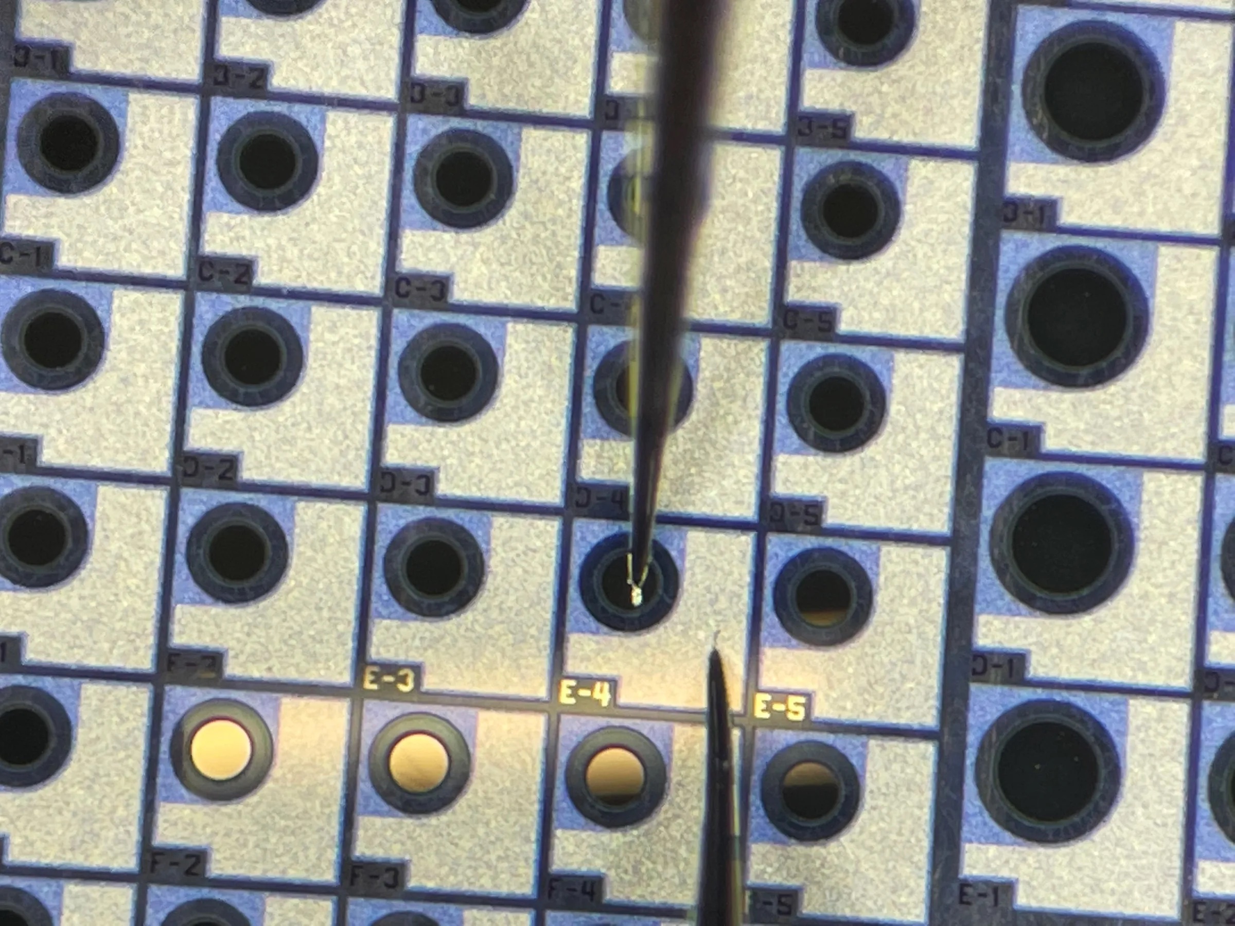
The IEDM paper describes the fabrication of a diode based on alloys of aluminum nitride capable of withstanding an electric field of 7.3 megavolts per centimeter—about twice as high as what’s possible with silicon carbide or gallium nitride. Notably, the device also had very low resistance when conducting current. “This is a spectacular result,” says IEEE Senior Member W. Alan Doolittle, a professor of electrical and computer engineering at Georgia Tech. “Particularly the on-resistance of this thing, which is ridiculously good.” The Nagoya paper has seven coauthors, including IEEE Member Hiroshi Amano, who won a Nobel Prize in 2014 for his role in inventing the blue LED.
“This is a new concept in semiconductor devices.”—DEBDEEP JENA, CORNELL
Aluminum nitride has long tantalized semiconductor researchers. One of the most important characteristics of a power semiconductor is its bandgap. It’s the energy, in electron volts, needed for an electron in the semiconductor lattice to jump from the valence band to the conduction band, where it is free to move around in the lattice and conduct electricity. In a semiconductor with a wide bandgap, such as gallium nitride (GaN) or silicon carbide (SiC), the bonds between atoms are strong. So the material is able to withstand very intense electric fields before the bonds break and the transistor is destroyed. But they both pale in comparison with AlN. The bandgap of AlN is 6.20 electron volts; for GaN it’s 3.40, and for the most common type of SiC, 3.26.
One longstanding problem with AlN is in doping, which is the insertion of impurity elements that give a semiconductor an excess of charges, thereby enabling it to carry current. Strategies for chemically doping AlN have only begun emerging in recent years, are not fully developed, and their effectiveness is a somewhat contentious subject among researchers. In doping, the excess charges can be electrons, in which case the semiconductor is referred to as “n-type,” or they can be electron deficiencies called holes, in which case it’s “p-type.” Nearly all commercially successful devices are made up of such doped semiconductors, sandwiched together.
But impurity doping, it turns out, is not the only way to dope a semiconductor. Some semiconductors based on a compound containing elements from group III and group V in the periodic table—for example the compound gallium nitride—have an unusual and remarkable property. At the boundary where two such semiconductors meet, they can spontaneously generate a two-dimensional pool of extremely mobile charge carriers, called a 2-dimensional electron gas, even without chemical doping. It arises from an internal electric field in the crystal, which comes from a couple of attributes. For one, crystals of these III-V semiconductors are unusually polar: Within the unit cells of the crystal, the clouds of electrons and positively charged nuclei are offset from each other enough to give every cell distinct negative and positive regions (a dipole). In addition, it’s possible to generate charges in the crystal lattice of these semiconductors simply by straining that lattice, a phenomenon called piezoelectricity.
The story behind the big advance
In the early 2000s, researchers at the University of California, Santa Barbara exploited these characteristics to develop a technique they called distributed polarization doping, which allowed them to get n-type doping of bulk (three-dimensional) gallium nitride without impurity dopants. The group included IEEE Fellow Umesh Mishra (now dean of engineering at UC Santa Barbara) and his graduate students Debdeep Jena and Huili (Grace) Xing, both now at Cornell University. Jena and Xing, both IEEE Fellows, later demonstrated p-type distributed polarization doping, in 2010, and then dopant-free 2D hole gases, in 2018, at Cornell.